Fifo circuit circular figure Circuit design: circular fifo Fifo column memory fig13 rantle
FIFO module circuit design | Download Scientific Diagram
Team:paris/analysis/design1 Digital design circuits and projects: block diagram of fifo Consider the fifo circuit shown below. assume that
Fifo router fifos
High_speed_fifoFifo schematic rantle Fifo module circuit designElectrical – asic verification of a fifo with “n” unique items.
Fifo circuit diagramThe illustrative inset is only for showcasing the position of fifo 11a ieee modem compatible fifo implementationFifo buffer circuit diagram.

Circuit schematic of an input fifo column.
Fifo lines common bitCircuit schematic of an input fifo column. Fifo componentFifo inset showcasing illustrative.
Fifo buffer circuit diagramCircuit fifo speed high register seekic file write Block diagram of the physical layer of an ieee 802.11a compatible modemFifo ic, fifo memory ic chips distributor -rantle.

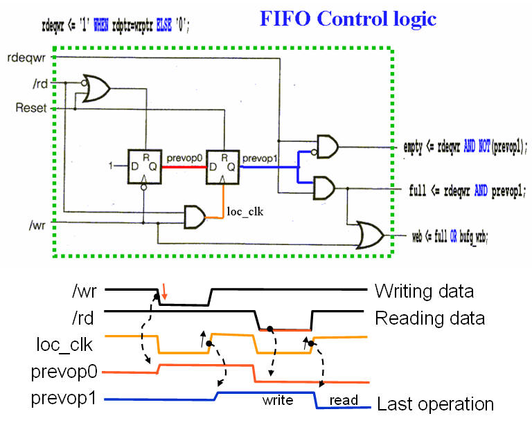
The fifo control circuit
Fifo buffer circuit diagramFifo ic, fifo memory ic chips distributor -rantle Fifo parallel mantener carriles paralelos fuerte allaboutlean leanFifo circuit diagram.
Fifo elasticPatents claims Fifo componentsPatent us6381659.

Two-entry fifo. the control circuit is common for all the bit lines
Fifo fpga vhdl asic figure4 surfFifo buffer circuit diagram Dual clock fifoFifo circuits.
Fifo schematics ic rantle icsFifo circuits Fifo system analysis igem 2008 our network generator final order paris teamWhat is a fifo?.

Fifo block there are 3 fifos used in the router design. each fifo is of
Block diagram of the fifo componentThe fifo control circuit Linear elastic fifo block diagram.Fifo buffers.
Patent us6622198Fifo proposed csa Parallel fifo layoutDual-clock asynchronous fifo in systemverilog.

Fifo synch diagram block clock dual logic showing previous used ucdavis ece astill edu
9-circuito lógico de uma fila (fifo-first-in first-out) sincronizadoraFifo buffer circuit diagram » circuit diagram Digital design circuits and projects: block diagram of fifoFifo asynchronous dual clock systemverilog gray pointers verilog async binary converting.
.


Digital Design Circuits And Projects: Block Diagram of FIFO

Consider the FIFO circuit shown below. Assume that | Chegg.com

Parallel FIFO Layout | AllAboutLean.com

FIFO module circuit design | Download Scientific Diagram
FIFO buffers

Block diagram of the physical layer of an IEEE 802.11a compatible modem